Crack Formation during Electrodeposition and Post-deposition Aging of Thin Film Coatings - 7th & 8th Quarterly Report
This NASF-AESF Foundation research project report covers the seventh and eighth quarters of project work (July-December 2017) on this AESF Foundation Research project at the University of Houston. The objective of the work is to study fundamental and practical aspects of crack formation in electrodeposited thin films.
#research #nasf
by
Prof. Stanko R. Brankovic*
Featured Content
University of Houston
Houston, Texas, USA
Editor’s Note: This NASF-AESF Foundation research project report covers the seventh and eighth quarters of project work (July-December 2017) on this AESF Foundation Research project at the University of Houston. Access information to past project reports referred to in this paper is listed at the end of this report. A printable PDF version of this report is available by clicking HERE.
Personnel:
- Stanko R. Brankovic, PI, Electrical and Computer Engineering and Chemical and Biomolecular Engineering, University of Houston,
- Kamyar Ahmadi, PhD Student, Material Science Program, University of Houston,
- Wenli Yang, PhD Student, Material Science Program, University of Houston.
- Omer Faruk Karadavut, MS student, Electrical Engineering Department, University of Houston
Objective
The objective of the proposed work is to study fundamental and practical aspects of crack formation in electrodeposited thin films. The aim is to identify and quantify the key parameters of the electrodeposition process affecting the crack formation in thin films. This study should enable development of an effective strategy generally applicable in practice whenever electrodeposition process for crack-free films is demanded.
The activities in this period were focused on identifying the advantage of a pulse deposition approach on the stress state of chromium thin films. The chromium films were deposited from Cr+3-containing electrolytes (EXDBA 1411 Bath with pH=5) using different pulse functions and their stress state was compared to the ones deposited with DC method.
Experimental approach
Upgrade of the stress measurement setup and noise reduction
The in-situ stress measurements during the pulse deposition of chromium films have been performed in an upgraded stress measurement system. The need for improvement and noise reduction was introduced by the nature of the pulse deposition process compared to that of DC deposition. The periodic change of current in an on/off cycle induced an additional level of noise in the in-situ stress measurements, which caused the cantilever to experience a higher level of noise/motion related to a perturbation of the deposition process. Therefore, the main noise source, related to the large absorbance of the solution and hydrogen bubble interference with the laser path from the back of the cantilever, had to be decreased. In order to be able to follow the stress change at the desired temporal resolution of different pulse functions and during the prolonged time of pulse current deposition, we redesigned our cantilever holder and added a new complexity in the system, with additional electrode placed in front of the cantilever surface on which the chromium film is grown (Fig. 1). The new cantilever holder closed up the distance of the back cantilever surface (reflecting surface) to the wall of the cell. This means that the path of the laser beam through the dark chromium solution was additionally shortened by ~ 1 mm total. The new holder also ensured that the laser beam reflection from the back of the cantilever was shifted to a lower position where significantly less hydrogen bubbles were trapped during chromium deposition and thus less interference with the laser path is achieved (Fig. 1(a)). The role of the additional mesh-electrode placed in front of the growing chromium film was to collect the maximum amount of hydrogen bubbles generated at the growing surface of chromium film, thus preventing them from migrating behind the cantilever and interfering with the laser path (Fig. 1(b)).
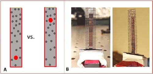
Figure 1 - (a) Relative position of the laser spot on the back cantilever surface in the new (L) and old (R) set up; (b) the position of the mesh electrode relative to the cantilever surface in the new set up, preventing the hydrogen bubbles from migrating behind the cantilever, and thus remaining trapped within the mesh and released to the surface of the solution without interfering with the laser path.
The improved set up was tested for an arbitrary length of ton for pulse functions of 50% duty cycle and jp =350 mA/cm2. The stress response of the system/cantilever was recorded (Fig. 2). As one can see, the new and improved set up is capable of providing measurements with real time resolution of the stress change during the pulse deposition. The compressive and tensile relaxation (d(F/w)/dt) during ton and toff is clearly seen in Fig. 2.
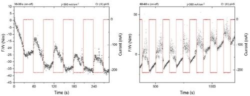
Figure 2 - Stress/Force per width measurements and system response during pulse deposition with the new experimental set up: (L) 30 sec / 30 sec pulse function, jp = 350 mA/cm2; (R) 60 sec / 60 sec pulse function, jp = 350 mA/cm2.
Pulse deposition
Deposition concept and pulse function design
In the previous reports we have shown that the pulse deposition approach leads to reduced tensile stress relaxation during the rest time, indicating a clear benefit when crack formation and the mechanical integrity of chromium films is considered during aging process. The pulse deposition design, in this case, was not introduced to mitigate the transport near the electrode surface nor to prevent Cr(OH)3 precipitation, but rather had an aim to effectively decrease the amount of Cr-hydride phase in the deposit and reduce the amount of dissolved hydrogen in the chromium lattice (Fig. 3). These two phenomena, as discussed previously (See Report #5 in the list at the end of this paper.), were identified as the main drivers for tensile stress relaxation in chromium films on deposition, and also as the main source for the compressive stress generation in chromium films during DC deposition. Therefore, the pulse function design was guided by the principal idea to have a DC-like process with periodic interruptions, i.e., off time, to allow the breakup of the generated hydride phase and permit permeation of the trapped hydrogen from the lattice to the free surface of the chromium film. The basic estimates of the pulse function assumed that, upon removal of the electrochemical driving force for hydride formation, (off stage of the pulse) the hydride break-up is an instant process much faster than the hydrogen-diffusion/permeation to the chromium-free surface. The solution of the diffusion equation assumed an approximate treatment using semi-infinite slab geometry, based on the idea that off time (toff) has to be long enough to allow ≈100% of the trapped hydrogen at the deepest point in the layer deposited in one pulse cycle (ton) to be removed by diffusion process. An approximate solution for this diffusion problem has the error function dependence:1

Here, the term x represents the thickness of the deposited layer in one pulse cycle for a given current, x = rt on where r is the deposition rate of chromium (1.5 ÷ 5 × 10⁻⁷ cm/sec) (Fig. 3). Using the literature value of DH for BCC metals as 5 × 10⁻⁵ cm-2∙sec-1,2 leads to the functional predicting the duration of toff as a function of the ratio between hydrogen concentrations at t = 0, and at t = toff, as:


Figure 3 - Schematic diagram of the pulse deposition function indicating the ton, toff and x parameters relevant to Equation 2. The light blue color/boxes in the figure indicate the hydride phase after deposition stage (ton) which is decomposed in the subsequent toff stage (light gray boxes).
Obviously, the accuracy of this estimate is largely a function of the C(toff)/Co ratio which satisfies the assumption for complete removal of hydrogen from the deposited chromium layer during the off time in the pulse cycle. The complete removal of hydrogen in a mathematical sense means Ct/Co = 0, which is not achievable in practice. Therefore, for the purpose of our experiments, we present in Table 1, the calculated values of toff based on the value of the inverse error function argument.

Table 1 - The toff time calculation as a function of the Ctoff/Co ratio for different ton values, according to Equation 2.
As one can see, the toff values are a function of (ton)2, multiplied by a constant that is a function of the desired hydrogen depletion in the growing layer during ton. These yield a variety of choices for the toff values shown in the Table 1, and it somewhat leaves a freedom of practical experimental design for the ton/toff ratio. In the present experiments, we show data that are obtained for the pulse function with a 50% duty cycle which falls into the desired range of Ctoff/Co and yet fulfilling the estimate of toff for a particular value of ton chosen to be 1 and 60 seconds.
DC vs. pulse deposition: qualitative and quantitative change of the stress state in the chromium film.
In Fig. 4 (Left), the force per width (F/w) transients during the DC deposition of a chromium thin film (j = 350mA/cm2) is presented for comparison purposes. As discussed in previous reports, a compressive stress relaxation is observed during the chromium thin film growth, which is attributed predominantly to the effect of Cr-hydride formation, hydrogen-incorporation into the chromium lattice and Cr-hydroxide incorporation into the film. This is a signature of the chromium deposition from a Cr(III) solution as opposed to a Cr(VI) solution, where the tensile relaxation is observed. On termination of the growth process, a tensile relaxation is observed. This is a result of Cr-hydride decomposition and subsequent volume change in the film, due to hydrogen permeation to a free surface, which is indirectly responsible for chromium thin film cracking during the aging process.
In Fig. 4 (Right), a F/w transient is presented during the pulse deposition of chromium film using the same current density and 50% duty cycle. This process can be considered as DC deposition interrupted by regular “off” growth stages, corresponding to the off time in the pulse function. The pulse time and off time are long, 60 sec each and therefore we do not consider this process to be optimized for any transport limitation alleviation but rather as a pulse deposition concept demonstrating the idea discussed previously. As one can see, the off time and on time during deposition is clearly visible with periodic F/w interruptions, where the compressive relaxation is related to the deposition part of the pulse cycle and tensile relaxation is related to the off time of the pulse cycle. The important result here is the overall trend of F/w over the time for the entire process. Instead of seeing an overall compressive relaxation, as in the DC process, pulse deposition, i.e., DC deposition with off time interruptions, leads to an overall tensile relaxation in the chromium films. This is qualitatively and quantitatively a completely different behavior than what is observed during DC growth. Indirectly, this means that the grain zipping process, which yields a tensile stress, is the dominant contribution to the overall stress state in the chromium film, while the hydride incorporation is indeed reduced with the introduction of the alternating off stage and where Cr-hydride decomposition and hydrogen removal is anticipated. Therefore, a pulse deposited chromium film from the Cr(III) bath qualitatively show same stress state as the DC films deposited from a Cr(VI) electrolyte.3
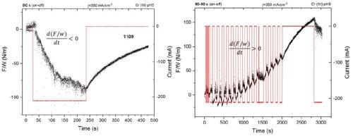
Figure 4 - Force per width (F/w) transients during chromium thin film growth from a Cr(III)-based electrolyte: (L) the F/w transient during DC growth and aging; (R) the F/w transient during pulse deposition growth and aging.
One more interesting result from this comparative experiment is that, although the DC deposited film thickness is about four times lower, it still shows about the same tensile stress increase (50 N/m) on aging compared to the pulse deposited film. Indirectly we can conclude that tensile stress relaxation is proportional to the amount of the Cr-hydride formed in the film which, in the case of the DC deposited sample is about four times more than in the case of the pulse deposited one. The long pulse time and off time in the experiment shown in Fig. 4 undoubtedly demonstrated the benefit of introducing the off stage in the DC-like type of deposition. In our further pursuit of this concept we purposely shortened pulse stage to 1 sec and kept the off-stage duration to 1 sec as well, while remaining within the boundary of the calculated parameters presented in Table 1. In this way, with this type of pulse function, we were approaching a more typical pulse deposition process, where some transport limitation related to the precipitation of Cr(OH)3 on the surface could be alleviated.
The pulse function in this form still does not represent any optimized form that should satisfy the conditions where no Cr(OH)3 forms on the surface, but this exercise should demonstrate if the shorter pulse forms do benefit the stress state in the chromium film, and whether the same qualitative change of the stress state in the film is preserved when compared to a DC-deposited sample. In Fig. 5, the F/w transients are shown for the pulse deposition process using jp = 350 mA/cm2 and a pulse function with a 50% duty cycle and ton = 1 sec. As shown in Fig. 5 (Left), the overall F/w trend shows a linear increase and positive stress change, i.e., tensile relaxation. For the first 200 sec of deposition or ≈ the first 150 - 200 nm, the F/w, i.e., the stress is negative, and then gradually changes to positive, and stays positive for the rest of the growth process. A higher temporal resolution of the measurement (Fig. 5 (Right)) shows that the pulse on and pulse off stages are still differentiated by the qualitatively different sign of the stress relaxation (d(F/w)/dt). Thus, in each pulse cycle we have subsequent hydride formation and hydride decomposition during the pulse on and pulse off stage, while the overall gain of stress during the thickening of the film is positive, i.e., tensile stress, about ≈ 80 MPa at 1-micron thickness.
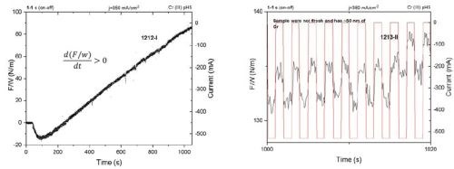
Figure 5 - Force per width (F/w) transients during the chromium thin film growth from a Cr(III)-based electrolyte: (L) the F/w transient during pulse deposition growth, 50% duty cycle; (R) higher temporal resolution of the results at left showing qualitatively different stress relaxation during the pulse on and pulse off time.
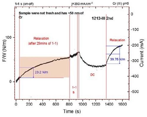
Figure 6 - Force per width (F/w) transients during chromium thin film growth from a Cr(III)-based electrolyte and during relaxation. The first 80 sec of the transient shows the end of the pulse deposition stage (ton/toff 1 / 1 sec, jp=350 mA/cm2), and then the film was allowed to relax for 750 sec. DC deposition, j=350 mA/cm2, was then initiated for 350 sec, and then the film was allowed to relax for 300 sec.
To explore further the effect of the shorter pulse function on the tensile relaxation during chromium thin film aging, an additional experiment was performed where the same thickness of chromium film was deposited using pulse deposition (ton/toff 1/1sec, jp=350 mA/cm2), and subsequent DC deposition. After each stage, the film was allowed to relax, while the stress relaxation was measured.
Data are shown in Fig. 6. The F/w transient during the pulse stage is not shown in its entirety due to a lack of the data collecting capacity of our system, but the full extent of the relaxation transient is recorded. The film was again briefly deposited, using pulse deposition before DC growth was implemented for the remaining time to produce a layer with the same chromium thickness. The film was then allowed to relax and the stress relaxation transient was recorded.
At an arbitrary point of 200 sec during the relaxation process, the stress relaxation is measured in each case, i.e., after DC deposition and after pulse current deposition. The tensile relaxation after pulse deposition, is a factor of two less than the tensile relaxation during DC deposition. As described before, this suggests that the amount of Cr-hydride and hydrogen trapped in the chromium matrix is about 50% smaller for the pulse deposition process. Considering that the pulse deposition function is not yet optimized to produce the chromium films with a minimum amount of Cr-hydride and trapped hydrogen, we consider this result as clear proof that the pulse deposition process of chromium films produces deposits with less aging stress as well as the different qualitative sign and value of the stress state during deposition. The question remains as to how short the pulse stage can be applied with same qualitative outcome, and whether the benefit of the pulse current approach can be extended to produce chromium films with less Cr(OH)3 phase incorporation. Our efforts are currently focused on this problem.
The different Cr-hydride content in the chromium films deposited using DC and pulse deposition approach was evaluated by following the surface morphology change over the time of deposition. The samples with ≈ 4-micron thickness were produced using both approaches, and the surface morphology was investigated using an optical microscope. The images at the same locations on the samples surface were taken immediately after deposition, then, after 1, 3 and 7 days. The results are shown in Fig. 7.
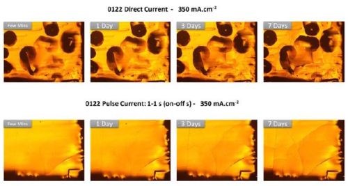
Figure 7 - The optical images of chromium thin film morphology during aging in air: (Upper row) the morphology of DC-deposited chromium films, j = 350 mA/cm2; (Lower row) the morphology of pulse-deposited chromium films, (ton/toff = 1 / 1sec, jp = 350 mA/cm2).
The DC-deposited samples show the typical blister-type of morphology which is a result of Cr-hydride break-up and entrapment of the resulting hydrogen gas that did not escape the chromium matrix immediately after the deposition process. With increasing aging time in air, the pressure builds up in the chromium films via hydrogen accumulation and a tensile relaxation. Thus, the first cracks start to appear at the bottom of the blisters, and then develop further into the rest of the film. For pulse-deposited samples, no blister morphology has been observed. The film surface appears smooth, but some initial cracks are immediately visible after the growth. As the aging progresses, the areal density of the cracks continues to grow, and cracks become more obvious. The chromium film cracks in the case of the pulse-deposited sample look qualitatively different than those developed in the DC-deposited chromium films. We believe that this is a good indication of the different stress state in the pulse-deposited films, which is mainly the result of the considerably lower amount of Cr-hydride formed during deposition process.
Conclusion
The pulse deposition concept studied in this period has been proven to be beneficial for changing the stress state in as-deposited chromium films. From mildly compressive stress typically seen in DC-grown chromium films, with pulse deposition approach, we can now routinely obtain films with a net tensile stress state. The pulse deposition function design was based on the aim of determining the off time of the pulse cycle such that a sufficient amount of Cr-hydride is decomposed, and the resulting hydrogen liberated in this process is allowed to permeate to the free surface. The preliminary data suggest that this can be achieved with different lengths of the pulse on/off time, and thus a more work is needed to determine a true optimum set of conditions. In the future, the efforts will be focused towards design of the pulse function that will incorporate the benefit of complete Cr-hydride removal and low Cr(OH)3 incorporation in the chromium films, both processes occurring over different time scales. Therefore, more theoretical work and experiments are needed; yet the data presented undoubtedly are encouraging and show that we are on the right path to design the process for the electrodeposition of functional chromium coatings from a Cr(III)-based electrolyte.
References
1. J. Crank, The Mathematics of Diffusion, 2nd Ed., Oxford Scientific Publication, New York (1979); p. 17.
2. D.A. Porter and K.E. Easterling, Phase Transformation in Metals and Alloys, Taylor and Francis, Boca Raton, FL (2004); p. 68.
3. J.K. Dennis and T.E. Such, Nickel and Chromium Plating, Butterworths, Toronto (1986); p. 176.
Past project reports
1. Quarter 1 (January-March 2016): Summary: NASF Report in Products Finishing; NASF Surface Technology White Papers, 81 (2), 12 (November 2016); http://short.pfonline.com/NASF16Nov2.
2. Quarter 2 (April-June 2016): Summary: NASF Report in Products Finishing; NASF Surface Technology White Papers, 81 (3), 14 (December 2016); http://short.pfonline.com/NASF16Dec2.
3. Quarter 3 (July-September 2016): Summary: NASF Report in Products Finishing; NASF Surface Technology White Papers, 81 (4), 12 (January 2017); http://short.pfonline.com/NASF17Jan2.
4. Quarter 4 (October-December 2016): Summary: NASF Report in Products Finishing; NASF Surface Technology White Papers, 81 (8), 16 (May 2017); http://short.pfonline.com/NASF17May2.
5. Quarter 5 (January-March 2017): Summary: NASF Report in Products Finishing; NASF Surface Technology White Papers, 81 (11), 12 (August 2017); http://short.pfonline.com/NASF17Aug1.
6. Quarter 6 (April-June 2017): Summary: NASF Report in Products Finishing; NASF Surface Technology White Papers, 82 (4), 10 (January 2018); http://short.pfonline.com/NASF17Jan1.
About the author

Dr. Stanko R. Brankovic is an Associate Professor in the Electrical & Computer Engineering and Chemical & Biomolecular Engineering Departments, as well as Associate Director, Center for Integrated Bio and Nanosystems at the University of Houston, Houston, Texas. He holds a B.E. in Chemical and Biochem. Eng. from the University of Belgrade, Serbia (1994) and a Ph.D. in the Science and Eng. of Materials from Arizona State University, Tempe, AZ (1999). He is active in many professional societies, including serving as Vice-Chair and member of the Electrodeposition Division Executive Committee of The Electrochemical Society (2006‐present) and as the Chair of the Electrochemical Material Science Division, The International Society of Electrochemistry (2012‐present). His research interests include electrodeposition, thin films, electrocatalysis, sensors, corrosion and electrochemical material science and nanofabrication.
*Corresponding author:
Dr. Stanko R. Brankovic
Associate Professor
Department of Electrical & Computer Engineering
Department of Chemical & Biomolecular Engineering
Department of Chemistry
N 308 Engineering Building 1
Houston, Texas 77204-4005
Phone: (713) 743-4409
Fax: (713) 743-4444
E-mail: srbrankovic@uh.edu
RELATED CONTENT
-
Qualitative Approach to Pulse Plating
In 1986, the AESF published Theory and Practice of Pulse Plating, edited by Jean Claude Puippe and Frank Leaman, the world’s first textbook on pulse plating. A compendium of chapters written by experts in this then-emerging field, the book quickly became the authoritative text in pulse plating. What follows here is the opening chapter, serving as an introduction to the field. Although the field has grown immensely in the intervening 35 years, the reader will find that the material remains a valuable introduction to those looking to advance the field of pulse plating.
-
Special Aspects of Electrodeposition on Zinc Die Castings
Electroplating is a frequent choice to give zinc die cast components a high-quality protective and decorative surface finish, however, applying this kind of treatment for die cast zinc components presents hidden challenges. In order to overcome these issues, a thorough morphology and composition analysis of die cast items was conducted. Special aspects of zinc die cast as a plating substrate are described and linked to the die casting process.
-
Chromium-free Etching and Palladium-free Plating of Plastics
Plastics are replacing metals in the manufacture of many parts, and quite often there is a need for metallic coatings on the plastics and other non-conductors. This paper will describe new processes of preparing ABS plastic substrates for subsequent metallization.


